

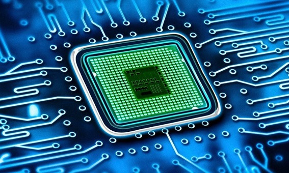
(Nanoelectronics _ Plasmonics) Application of nano-plasmonics in the construction of integrated circuits and other electronic devices
Researcher and author: Dr. ( Afshin Rashid)
Note: High-velocity plasmon nanoparticles with a half-step resolution of 22 nanometers are concentrated using relatively low-diffusion surface plasmons through relatively low-diffusion surface plasmons and later converted to localized plasmons. This allows highly efficient transmission and near-field focus, which is the key to improving power for a given laser power, by increasing the scanning speed and / or using a number of parallel patterns.
In essence, high-velocity plasmon nanoparticles with a half-step resolution (22 nm) allow us to produce nano-electronic devices that can create 12-inch wafers in minutes. This is comparable to conventional photolithography at the production level but at a much higher resolution than the 22 nm half-step size. This new design enables low cost, high-performance nano-scale maskless production with several times higher power than conventional maskless methods. Using shorter wavelengths of plasmon nanoparticles and conduction mechanisms, it is possible to increase the continuous scale to a nodule size of less than 22 nanometers, opening a promising path for next-generation lithography to produce semiconductors. In addition, in next-generation magnetic data storage, known as nano-electron-assisted nano-electronics devices and devices, it has the potential to be twice as powerful in the future.

The application of nano-lithography is the fabrication of integrated circuits and other electronic devices in which optical lithography is widespread. In addition, various types of nano-lithography techniques are used in research activities with the aim of modeling materials and realizing prototypes and concept proof devices. Methods of application of nano-lithography on a spin substrate Due to the specific interactions between these polymers and the substrate , in certain conditions, two types of polymers tend to create an intertwined pattern, there is a local order between both polymers and amplitudes. It forms a nanowire with a period in the range of 50 nanometers. This pattern will be very useful if the subsequent application of nanolithography , which after landing on the layer due to less penetration mobility, tends to accumulate on top of the polymer. Thus the thin bottom structure follows the polymer scaffold, which expands smoothly along different microns. However, the formed nanowires reveal some unwanted features as a closer look. Significant unevenness is observed in the fabrication of nanowires, also the nanowires are cut at certain points and deviate from the direct shape, which They are all typically the source of the deteriorating physical properties of nanowires. In addition, long-distance ordering of fabricated nanowire arrays does not follow this strategy, which is essential in certain applications such as the semiconductor industry.

Conclusion :
High-velocity plasmon nanoparticles with a half-step resolution of 22 nanometers are concentrated using relatively low-diffusion surface plasmons through relatively low-diffusion surface plasmons and later converted to localized plasmons. This allows highly efficient transmission and near-field focus, which is the key to improving power for a given laser power, by increasing the scanning speed and / or using a number of parallel patterns.
Researcher and author: Dr. ( Afshin Rashid)
PhD in Nano-Microelectronics